
Combinatorial approach for discovery of emerging alloys for various applications
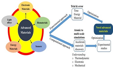
The need for better quality sustainable lifestyle with higher demands in the modern world pushes for the development of new materials from the available resources with superior functionalities and outputs. In this pursuit, my research focuses on the development of novel alloys with enhanced properties. This idea is standing on three main pillars of materials science and engineering:
Alloy design through synthesis and its further processing: Combining different elements to synthesize alloys needs a faster approach. Combinatorial approach, synthesis of different compositions of fixed number of elements in one step, is a way to produce all alloy compositions quickly. My research concern is to develop alloys through electro-deposition and powder metallurgy using combinatorial approach. Further, all alloys produced could develop improved properties with their processing. Several post materials processing routes (thermal/mechanical/thermo-mechanical treatments) are formalized and the phase transformations with the associated properties of the alloys are studied.
Microstructure characterization of the designed alloys: Alloys after their synthesis and processing consist of either various crystallographic phases with different crystal orientation arrangements (polycrystalline) or are of amorphous character (metallic glass). Since all these characteristics directly affect its functional properties, the research work will also include comprehensive study of phase and microstructure of the developed alloys. Generally, X-ray diffraction is used for phase and crystal orientation (texture) determination and electron microscopy would be utilized mainly for microstructure characterization.
Properties determination of the designed alloys: To select-out the alloy of interest, the structural and/or functional properties of the designed alloys are determined using various scientific equipment/tools for eg, tensile testing machine, biocompatibility, solar IV characteristics, etc.
(A) Functional Applications
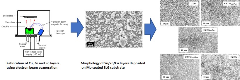
(1) Synthesis of CZTSSe thin films through electron beam evaporation (Mr. P.K. Kannan):
Copper Zinc Tin Sulfide (CZTS) is prominent photon absorber layer in thin film solar cell. This work involves fabrication of CZT metallic precursors through sequential electron beam evaporation of the elemental metallic precursor layers, which upon sulfo-selenization lead to the formation of CZTSSe films.
Electron beam evaporated metallic precursors are sulfurized in different environments to form CZTS(Se) films. The effect of various annealing parameters on the structural, optical and morphology are investigated. Films sulfurized in presence of elemental S powder is found structurally superior.
Research highlights:
Received prestigious SERB-Purdue University Overseas Visiting Doctoral Fellowship to carry out research in Prof. Rakesh Agrawal's research lab in Purdue University, IN, USA from Jan to Dec 2019.
Received Research Excellence Award from IIT Hyderabad for 3 consecutive years from 2015 to 2017.
Selected Publications:
Detailed Investigations on Influence of Precursor stacking and Sulfurization for Cu2ZnSnS4 film formation.
Kannan P.K., Sushmita Chaudhari,Suhash R. Dey (2018), Thin Solid Films, Volume 649, 2018, 81-88, https://doi.org/10.1016/j.tsf.2018.01.038.
Impact of sulphurization environment on formation of Cu2ZnSnS4 film using electron beam evaporated stacked metallic precursors.
P.K. Kannan, Sushmita Chaudhari and Suhash R. Dey, Bulletin of Materials Science, Volume 42, 2019, pp.11-17, https://doi.org/10.1007/s12034-018-1726-8
(2) Copper Indium Gallium Selenide (CIGS) absorber layer fabrication for solar photovoltaic applications
CuInxGa(1-x)Se2 is prominent material for solar photovoltaic applications due to its high solar to electricity conversion efficiency, reliability and stability.
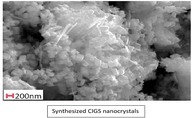
(a) Through CIGS nanoparticles deposition (Ms. Madhuri K.):
CIGS nanoparticles plays a crucial role in absorber layer due to its high surface to volume ratio and for requirement of low processing temperature. The post treatment of absorber layer by Intense Pulsed Light (IPL) gives highly crystalline CIGS films using its constituent particles. The proposed process is non-vacuum based performed at room temperature without selenization treatment. The construction of composition grading profile and patterning of CIGS layer on Mo/SLG enhances the charge collection efficiency and maximizes the solar spectrum absorption.
Selected Publications:
- Effect of Annealing duration and Heat flux on solvothermal synthesis of CIGS nanoparticles.
Madhuri K, Kannan P.K., Sushmita Chaudhari, Sanjay R Dhage, Suhash R. Dey (2018), ISFM-2018, International Symposium on Functional Materials, Chandigarh, India, Materials Today: Proceedings, Volume 21, pp. 1856-1861, https://doi.org/10.1016/j.matpr.2020.01.245
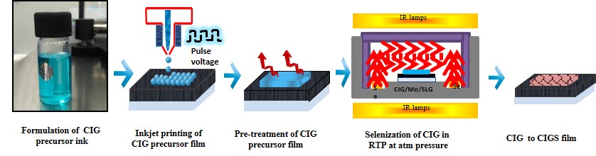
(b) Through Inkjet printing (Mr. Brijesh Singh Yadav):
CIGS thin film absorber layer is crucial for high efficient thin film solar cells because of its Cu(In, Ga)Se2(CIGS) solar absorber materials have gained market attention for thin film solar cell applications due to their high absorption coefficient(105/cm), tunable band gap, long term stability and high efficiency. Recently, CIS thin film solar cell demonstrated 22.9% efficiency on lab scale achieved by solar frontier and it seems to be most promising alternative to silicon solar cells. Non-vacuum techniques (spin coating, doctor blading, inkjet printing and electrodeposition) for formation of CIGS absorber layer is always favored for its cost effectiveness over the vacuum based routes. Among non-vacuum routes, inkjet printing has highest material utilization due to which it can significantly reduce the processing cost of CIGSe2 thin film solar cell by minimizing the consumption of materials (In, Ga) during deposition. The most challenging issues that remain open for the fabrication of CIGSe2 absorber layer via inkjet printing are: (1) formulation of long term stable precursor ink, (2) Influence of jetting and printing parameters (3) effect of atmospheric processed selenization on quality of absorber layer without using reactive H2Se/H2S sources. In this context, we formulated precursor ink in aqueous medium that showed stability more than a month. Preparation of ink consists of metal nitrates precursors dissolved in DI water along with PEG (Polyethylene glycol) to obtain stable jetting droplet. We tailored the jetting and printing parameters to print uniform and pinhole-free precursor layer on Mo coated glass substrate. Multiple printing was done in order to achieve desired thickness of the precursor film which was further selenized in RTP (Rapid thermal process) furnace under selenium rich atmosphere. Fine tuning of selenization process led to highly crystalline, dense and crack free CIGS film confirmed by XRD, RAMAN and FESEM techniques. C-V characteristics showed that the film has p-type semiconducting properties with carrier concentration of 1016/cm3. Finally, CIGSe2 device fabricated by sequential deposition of CdS (n-type), i-ZnO, and Al:ZnO layers. Based on high quality CIGS absorber layer, pure selenide CIGS solar cell with a photoconversion efficiency of 5.2% has been achieved on active area of 0.18 cm2 under AM1.5 solar irradiation. Still, more fine tuning of selenization process is required to improve the CIGS absorber layer quality and decrease the MoSe2 thickness.
Selected Publications:
Chalcopyrite CIGS absorber layer by inkjet printing for photovoltaic application.
Brijesh Singh Yadav, Suhash Ranjan Dey, Sanjay R.Dhage (2017), 2nd International Conference on Solar Energy Photovoltaic, Bhubaneswar, India, Materials Today: Proceedings, Volume 4, 2017, 12480-12483, https://doi.org/10.1016/j.matpr.2017.10.047.
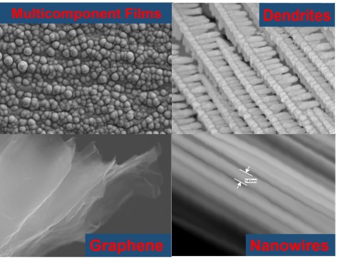
(3) Morphological and topographical studies of novel alloy materials electrodeposited by random and/or constrained growth for practical applications (Dr. Chokkakula L. P. Pavithra, Mr. Siri Kiran Reddy)
The surface of metals or more precisely the interface at the metal/environment plays a significant role in property establishment and ultimately the application of a material. Multicomponent alloys having more than 4 elements have been proven to be good materials on account of reduced corrosion and high strength. Conventional methods are not only limited in terms of tailoring the product but are also very costly. Electrodeposition becomes an economically viable and better alternative as a thin film can be grown on any shapes and bulk processing is not required. The present work is to study the growth of these films in aqueous solutions.
(B) Structural Applications
(1) SLM 3D Printing of 17-4 PH SS & its surface modification for biomedical implants
The planned work aims to find an alternative approach to replace the commercially present expensive biomedical implants used for orthopedic applications by employing SLM 3D printing techniques of 17-4 Precipitation Hardened Stainless Steel. The primary objective is to make the implant structure porous to reduce it's EM and reduce the stress shielding effect of the implant. The secondary objectives include surface modification of the implant for excellent corrosion resistance, cell growth and superior biocompatibility within the body fluid environment in contrast to the already available biomedical implants.
The work is carried out between IIT Hyderabad, India & Swinburne University of Technology, Melbourne as a candidate for partnered Ph.D. program between both the institutes
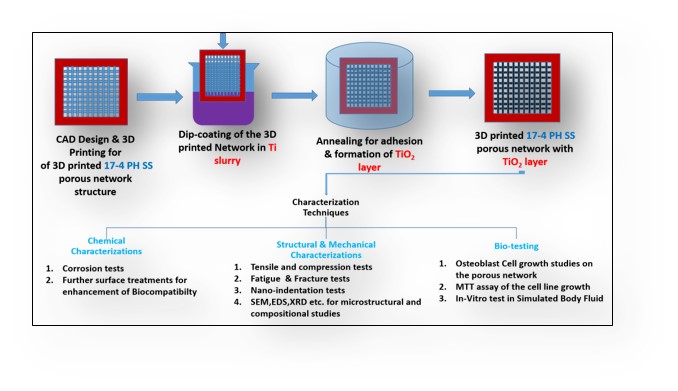
Web link: A possible solution to reduce stress shielding effects in cost effective manner