Research Facilities
In case you would like to use any of the equipments or optical setups, please send an email to shourya@msme.iith.ac.in.
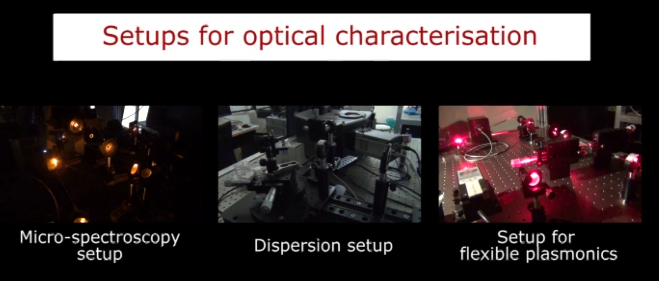
Optical setups in the labs (Video)
Optical spectroscopy setup
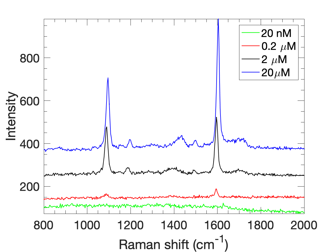 (left) Optical setup (right) Raman spectrum of mercapto benzoic acid (MBA) using 1 mW power and 1 sec. integration time.
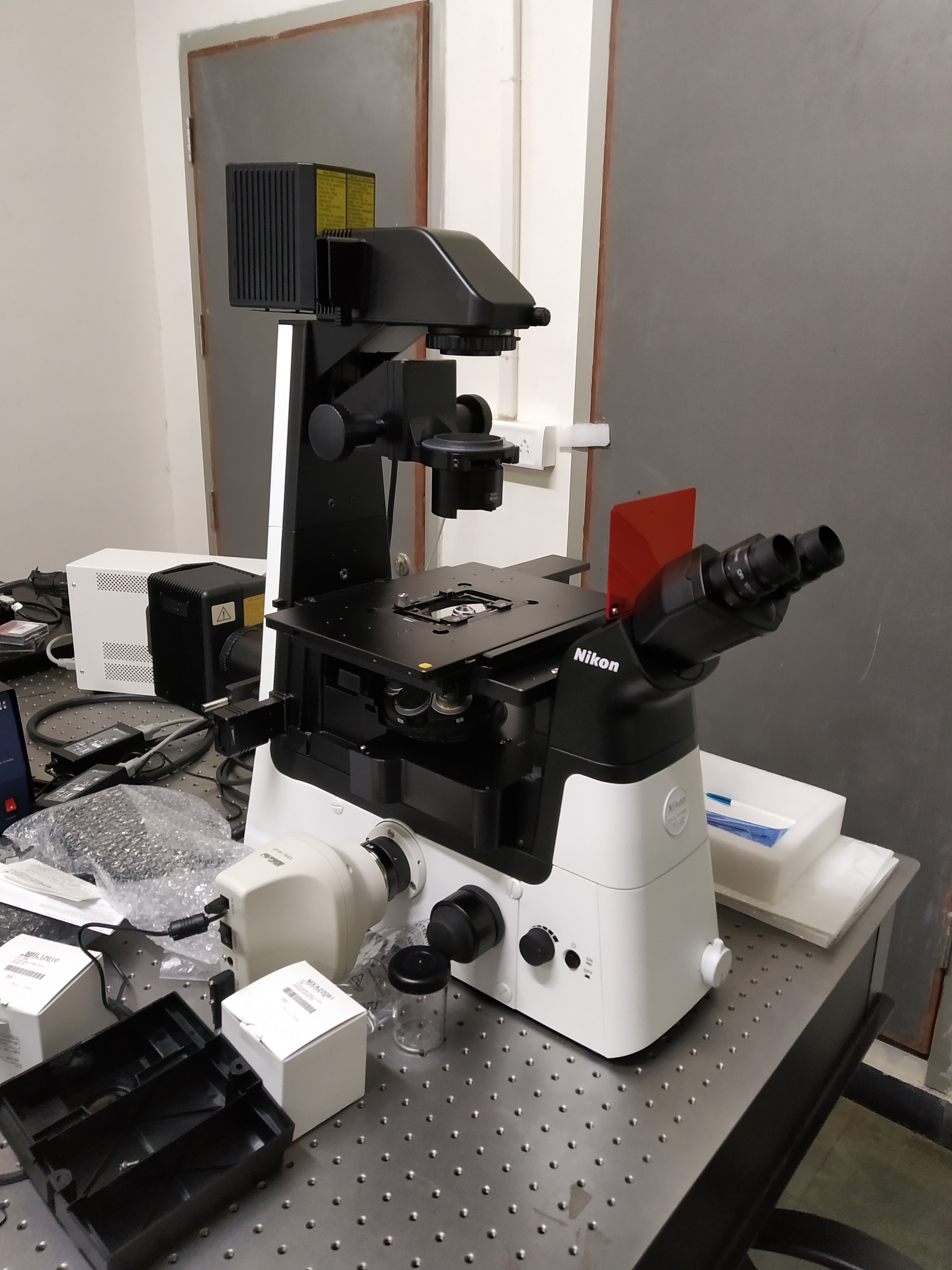
We have a assembled a micro-spectroscopy setup by coupling an inverted microscope (Nikon Ti2U) to a spectrometer (Andor Kymera 328i with Newton 920 CCD). The system is capable of the following measurements
- Bright-field transmission/reflection spectroscopy
- Dark-field transmission spectroscopy
- Raman spectroscopy (single point & time dependent)
The typical working range of the setup is
- Wavelength: 400-1000 nm
- Gratings: 150 l/mm, 600 l/mm, 1200 l/mm, 2400 l/mm
- Raman laser wavelength & power: 594 nm & 100 mW
- Raman spectroscopy range: 250 cm-1 to 3500 cm-1
Lab: MSME-111, IIT Hyderabad
DC Sputtering System
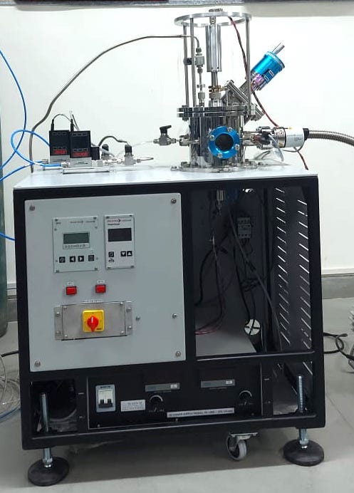

A DC sputtering system is available for the deposition of conducting materials with thickness upto 1 micron. The system has a 1 kW power supply enabling the deposition at a varying ranges of power. We also have the option of carrying out the deposition in the presence of different gases like Ar and O2.
The typical working range of the setup is
- Materials: ITO, Ag, Cu, Au
- Thickness: Upto 1 micron
- Gases: Ar, O2, N2
Lab: MSME-111, IIT Hyderabad
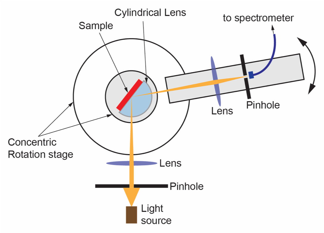
Dispersion measurement setup
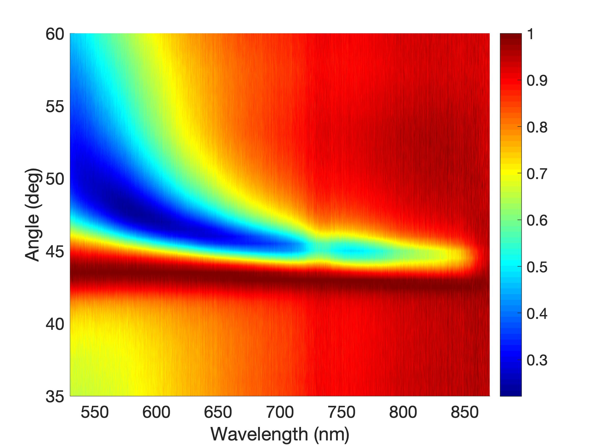 (left) Dispersion setup (right) SPP dispersion on 60 nm gold film.
We use this home-made setup for measuring the dispersion diagram (reflectivity vs wavelength and angle of incidence) of surface plasmons. The setup consists of a theta-2theta stage from Holmarc which supports the cylindrical lens and sample of interest. White light illumination from a halogen source is directed to the sample using standard optical elements and the reflected light is analyzed using a spectrometer.
The working range of the equipment is
- Wavelength: 500-850 nm
- Angle: 30 deg - 70 deg
This setup can also be used for measuring the angular optical response of thin film multi-layer samples.
Lab: MSME-111, IIT Hyderabad
Optical spectroscopy setup with in-situ heating
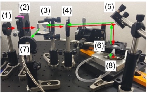
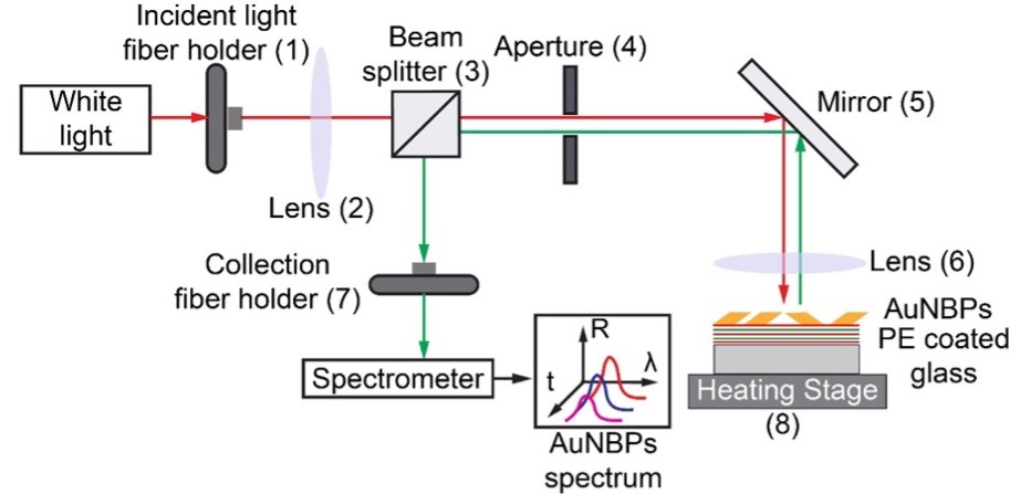 (left) Optical setup for carrying out in-situ heating experiments (right) SPP dispersion on 60 nm gold film.
A home-made optical setup for measuring reflection spectrum (from 400-900 nm) as a function of temperature is available. A white light illumination from a halogen source is directed to the sample using standard optical elements and the reflected light is analyzed using a spectrometer (Andor Kymera 328i with Newton CCD). This system can be used for tracking any temperature dependent changes in the optical response. We can currently carry out the heating experiments under atmospheric conditions. However, we are developing a new heating stage to carry out the experiments under vaccum or a controlled atmospheric condition.
Lab: MSME-111, IIT Hyderabad
Top-down nanofabrication
We have the necessary knowhow to fabricate nanostructures using shadow-sphere lithography (SSL) and focused ion beam (FIB) lithography.
Using SSL, we can fabricated nanoaperture structures from 80 nm to around 900 nm in size. This is mainly governed by the size of the silica particles used as the mask. With FIB, variety of samples with dimensions down to 40 nm can be fabricated.
Lab: MSME-410 and C-Annex (FIB), IIT Hyderabad
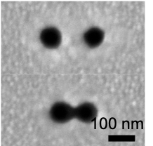
Chemical synthesis of nano- and micro-particles
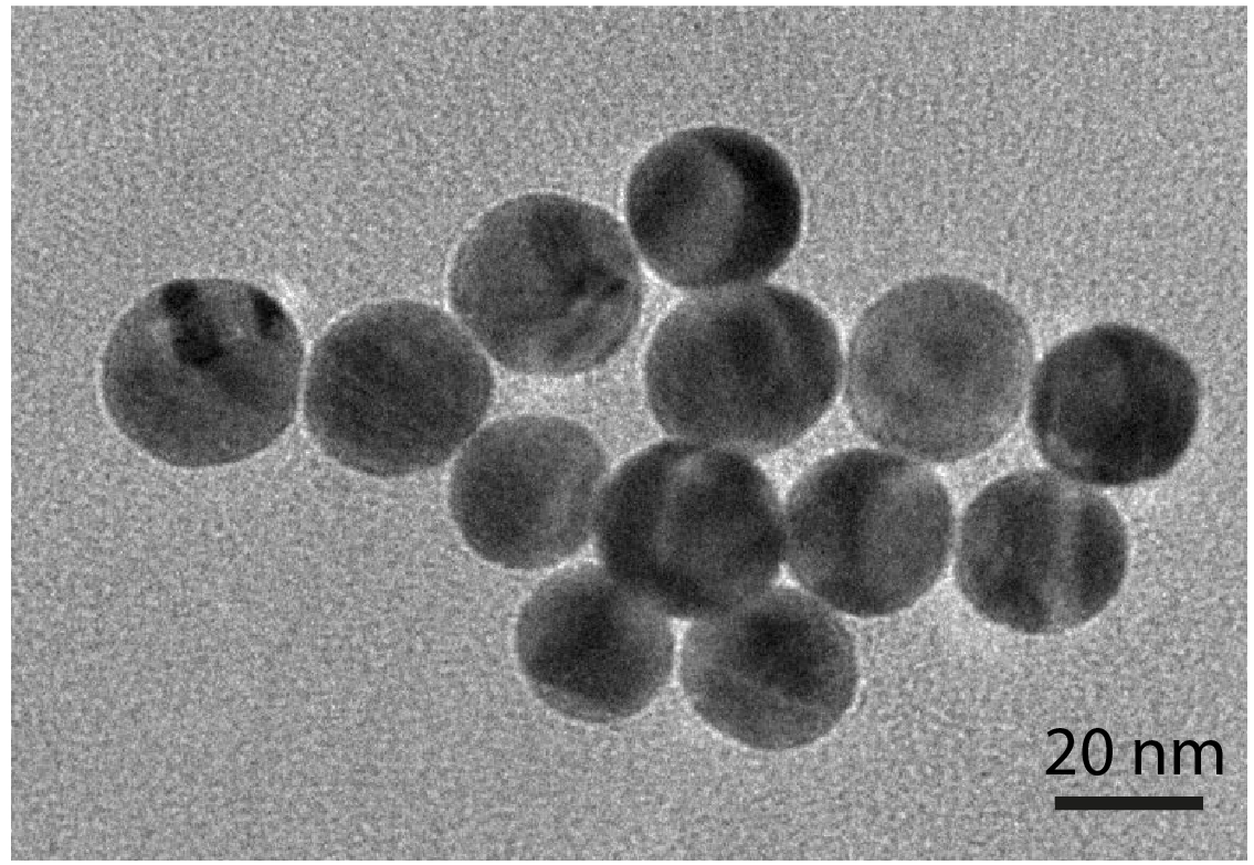
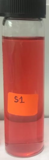
The necessary facilities for synthesis of gold, silver and silica particles with different shapes/sizes are available in lab. We typically characterize the synthesized particles using techniques like UV-Vis spectroscopy (available as a common facility), DLS (available in the institute), SEM (available as a common facility) and TEM (available as a common facility).
At present, we have the protocols for preparing the following particles:
- Gold nanospheres, nanorods, nanobipyramids, nanoplates
- Silver nanospheres and nanowires
Lab: MSME-410, IIT Hyderabad
Micro- and milli-fluidic devices
PDMS based micro- and milli-fluidic channels are fabricated for lab-on-a-chip based devices for fast and label free detection of analytes. We have developed various protocols for making low-cost 3D printed mold patterns for different micro- & milli-fluidic devices.
Lab: MSME-410, IIT Hyderabad
Other equipment in the lab
- Digital oscilloscope
- Function generator
- DC power supply
- Laser power meter
- 3D printer (Ender 3)
- Centrifuge
- Microcentrifuge
- Microbalance
- Stereo microscope
- Spincoater
- Hot plate with magnetic stirring
- Vortex
- Syringe pump
- Oven
- Dip coating setup (homemade)
Common facilities at IIT Hyderabad
- Focussed ion beam (FIB)
- Magnetron sputtering machine
- Transmission electron microscope (TEM)
- Scanning electron microscope (SEM)
- Confocal Raman microscope
- UV-Visible spectrometer
- X-ray diffraction (XRD)
- Atomic force microscope (AFM)